| Common apparatus |
|---|
| Hydraulic system |
| Electronic components |
| Data acquisition |
| EMG monitoring |
| NLID Tools |
| Troubleshooting |
| Materials |
| Supine apparatus |
|---|
| Assembly procedure |
| Safety Measures |
| Components |
| Servovalve |
| Actuator |
| Potentiometer |
| Pressure Filter |
| Torque transducer |
| Boot |
| Literature |
| Computing resources |
|---|
| CVS |
| Ethics |
|---|
| SDS / Inventory |
|---|
Delsys® Electrode Tester
Functional Description
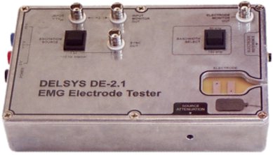 This device allows
one to drive a Delsys® DE-2.1 EMG electrode with waveforms to evaluate the
performance of the electrode and attached Bagoli™ amplifier unit.
This device allows
one to drive a Delsys® DE-2.1 EMG electrode with waveforms to evaluate the
performance of the electrode and attached Bagoli™ amplifier unit.
The electrode/amplifier combination will henceforth be referred to as the DUT
- device under test.
The DUT's step response may be measured by using the square-wave oscillator internal to the tester. The SYNC OUT connector outputs a large-signal square wave suitable to trigger a measuring device (e.g., oscilloscope) so that an ensemble average of the system response may be obtained.
The user may also drive the DUT with an arbitrary waveform by selecting the external excitation source. External inputs should be approximately 1V peak-to-peak. The INPUT MONITOR OUT connector provides a buffered version of the input but scaled by 2. This is to compensate for the factor of two gain that occurs when the test signal is converted to a differential electrode drive. (Incidentally, in principle it should have been possible to obtain the step response of the DUT by applying an external square wave from a function generator. However, upon closer examination, the generator in the lab was found to produce lousy square waves. The signal generated internally by the tester is of better quality.)
The BANDWIDTH SELECT switch sets the bandwidth of the tester to either 50 kHz or 150 kHz. (Approximate values. See performance tests below.) The smaller bandwidth is suitable when measuring sinusoidal response, as it will produce a slightly cleaner signal, whereas the larger bandwidth should be used when testing step responses. Note that with BW SELECT set to 50 kHz that the magnitude frequency response of the DUT may be evaluated up to 8 kHz with a maximum error of 0.1 dB; at this frequency the phase frequency response will have an error ~ 10 deg. (See this tester frequency response.)
The SOURCE ATTENUATION adjustment allows one to attenuate the electrode drive into the low mV level.
The ELECTRODE MONITOR OUT connector taps directly off of one of the two electrode excitation pads.
The ELECTRODE REFERENCE must be connected to the DUT electrode reference lead.
Schematic
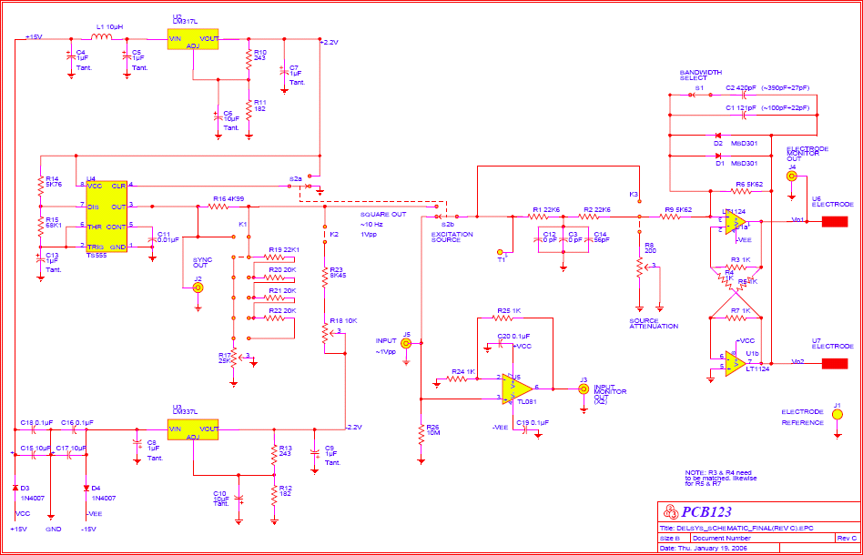
The above schematic is available in PDF format and in its original PCB123 format.
List of Components
- LM317L Positive voltage regulator, adjustable
- LM337L Negative voltage regulator, adjustable
- LT1124 Operational amplifer, Dual, low-noise, precision
- MBD301 Schottky barrier diode
- TL081 Operational amplifier, Wide bandwidth JFET input
- TS555 Timer, Low power CMOS
- Parts List (Excel)
Circuit Description
Multivibrator Circuit
The internal square wave test signal is generated by U4, a 555-based multivibrator that is enabled when CLR is tied HIGH via switch S2. The square wave frequency is 10 Hz (48% duty cycle) and of amplitude 0-2V. All values are approximate. See p. 9 of TS555 data sheets for design equations. The output of U4 is made available to the user as an external trigger signal.
The circuitry downstream expects a signal of 1Vpp. Resistors R16-R22 and the -2.2V supply circuitry (U3, R12, R13, C8, C9, and C10) condition the raw pulse-train from U4 so that it spans ±500 mV at test point T1. The position of jumper K1 and settings of trim pots R17 and R18 are iteratively adjusted until the required signal profile is obtained at T1. (Except for the first jumper position of K1, which bypasses R16 and is intended for circuit debugging, the remaining lower positions select different attenuation ranges in order to accommodate the variability in output voltage between different timer chips. Note that it will not be possible to condition the raw pulse-train in the case where U4 generates an output that spans 0.35 - 1.5V, which is an extreme scenario.)
Power Supply
Because the electrode drive is to be in the millivolt range U4 is powered with a low-voltage supply (+2.2 V) generated by programmable voltage regulator U2, R10, R11, C6, and C7. See p. 6 of the LM317L data sheets for design equations.
It was experimentally found that when U4 is powered with +5V that obtaining a clean attenuated electrode-drive signal was very difficult. Lowering the supply voltage helped.
C4, L1, and C5 form a pi-filter to de-couple switching transients at U4's VCC pin from the main +15V supply.
Differential Drive Circuit
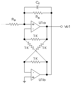
U1, R3-R7 and R9 convert a single-ended input voltage into a differential electrode drive. Since vo1 = -vo2 this circuit effectively provides a gain of 2. Schottky diodes D1 and D2 limit the output voltage of vo1 and vo2 to about ±400 mV; under normal operation these dioes are off. Capacitors C1 and C2 limit the bandwidth of the circuit. In order to understand how this circuit operates with the rest consider the following circuit snippet.
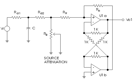 The
circuit shown here captures the key elements of the EMG electrode tester. vi
may come either from the multivibrator circuit or be an external input supplied
by the user. Rd1 represents the source resistance of vi. The remaining components
relate to actual components in the above schematic in a straight forward manner.
The
circuit shown here captures the key elements of the EMG electrode tester. vi
may come either from the multivibrator circuit or be an external input supplied
by the user. Rd1 represents the source resistance of vi. The remaining components
relate to actual components in the above schematic in a straight forward manner.
The system transfer function is as follows,
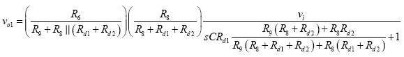
which describes a 1st-order low-pass system with time constant ![]() .
For the specified component values the following approximation may be
made, since R8 << Rd1 and R8 << Rd2:
.
For the specified component values the following approximation may be
made, since R8 << Rd1 and R8 << Rd2:
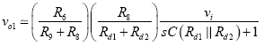
Since R6 = R9 the circuit can only attenuate the input. If Rd1 = Rd2 = 22k6 then the gain of the system (vo1/vi) ranges from [0, 0.004].
Capacitance C may be used to limit the bandwidth of the circuit, but at present it plays no significant role. If S2 is set to pass through the pulse train then the worst case value for Rd1 = R1 + (combination of resistors R16-R23 at their maximum value). Hence, the range of Rd1 is 22k6 to 26k2 ohms. Since Rd2 = 22k6 and C = 56pF, the circuit has a break frequency of greater than ~23 MHz. On the other hand, if S2 is set to pass the signal applied at connector J5 then the source resistance would have to be greater than ~3600 ohms to create a lower break frequency.
 Consider
now the effects of placing the capacitance Cf in parallel with R6, as shown
in this figure. The resulting approximate transfer function is,
Consider
now the effects of placing the capacitance Cf in parallel with R6, as shown
in this figure. The resulting approximate transfer function is,
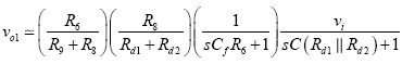
which shows that Cf introduces another pole in the system (at s = - Cf
R6) and may be used to limit the system bandwidth and reduce ouptut noise.
Debugging
Measuring the frequency response of the differential stage (U1)
Move jumper K3 into upper position. This applies the input signal directly to the input of the differential stage. Input signals should be limited to pear amplitudes of ~100 mVpp to avoid activating D1 and D2.
Tester Performance
Frequency Response Between INPUT and INPUT MONITOR OUT
This frequency response was measured using a Hewlett-Packard HP3562A dynamic
signal analyzer (sinusoidal source excitation, 1 Vpp) with the tester box
set for minimum attenuation.
As expected the gain is 2 and flat to beyond 100 kHz. (Theoretically
the magnitude response should be flat to > 1.25 MHz.)
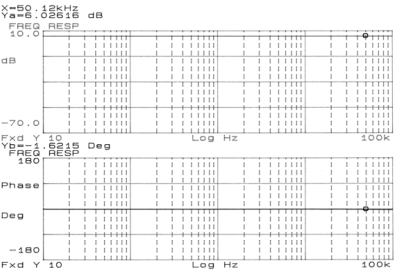
Frequency Response Between INPUT and ELECTRODE
MONITOR OUT
(50 kHz BW Setting)
This frequency response was measured usign an HP3562A dynamic signal analyzer
(sinusoidal excitation source, 1 Vpp) with the tester box set for minimum
attenuation and BW SELECT = 50 kHz.
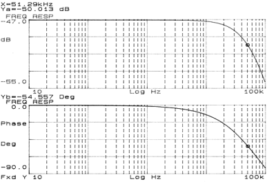
The measured BW = 51 kHz. The usable range for determining magnitude frequency
response of the electrode system is 8 kHz, at which point there is a maximum
gain error of 0.1dB.
Frequency Response Between INPUT and ELECTRODE MONITOR OUT
(150 kHz BW Setting)
The frequency limit of the HP3562A dynamic signal analyzer is 100 kHz. As such, it was not possible to obtain a frequency response plot for the tester at this BW setting. Instead, the cut-off frequency was determined using a function generator and an oscilloscope and finding the -3 dB point. It was experimentally determined that the actual BW is 141 kHz; measured with a sine wave input of 1 Vpp and the tester set to minumum attentuation.
Internal Square-Wave Output
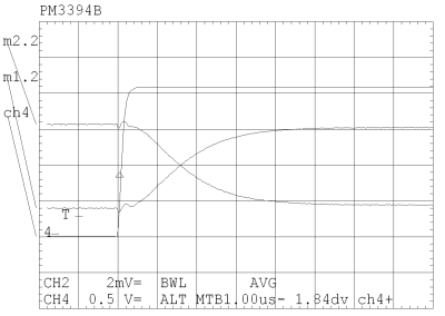 Output
traces of SYNC OUT (ch4, 500 mV/div) and both electrode excitation pads
(m1.2 & m2.2, 2 mV/div) after 512 averages. Timebase = 1 µV/div.
Tester was set to minimum attenuation and BW SELECT = 150 kHz.
Output
traces of SYNC OUT (ch4, 500 mV/div) and both electrode excitation pads
(m1.2 & m2.2, 2 mV/div) after 512 averages. Timebase = 1 µV/div.
Tester was set to minimum attenuation and BW SELECT = 150 kHz.
Risetime of electrode excitaiton signals ~ 2.6 µs.
A glitch correlated with the SYNC OUT edge is evident on the excitation signals.
The size of the glitch is ~450 µVpp when attenuation is minimal.
(Several attempts were made to remedy this situation but to no avail.)
Glitch Baseline
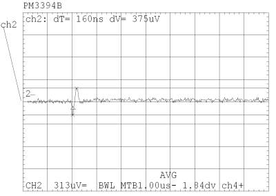 Output
from ELECTRODE MONITOR OUT when source attenuation is maximum (i.e., 0 V
out.) Glitch correlated with SYNC OUT has magnitude ~375 µVpp. (512
averages taken.)
Output
from ELECTRODE MONITOR OUT when source attenuation is maximum (i.e., 0 V
out.) Glitch correlated with SYNC OUT has magnitude ~375 µVpp. (512
averages taken.)
Small Signal Output
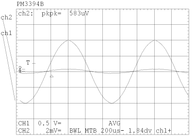 Output
from INPUT MONITOR (Ch 1) and ELECTRODE MONITOR (Ch 2) for a 1 kHz 1 Vpp
sine wave in with high source attenuation and BW SELECT = 50 kHz. After
512 averages the output is a sine wave of ~580 µVpp with no obvious
distortion.
Output
from INPUT MONITOR (Ch 1) and ELECTRODE MONITOR (Ch 2) for a 1 kHz 1 Vpp
sine wave in with high source attenuation and BW SELECT = 50 kHz. After
512 averages the output is a sine wave of ~580 µVpp with no obvious
distortion.
Last modified: 2006-09-04 Ross Wagner