| Common apparatus |
|---|
| Hydraulic system |
| Electronic components |
| Data acquisition |
| EMG monitoring |
| NLID Tools |
| Troubleshooting |
| Materials |
| Supine apparatus |
|---|
| Assembly procedure |
| Safety Measures |
| Components |
| Servovalve |
| Actuator |
| Potentiometer |
| Pressure Filter |
| Torque transducer |
| Boot |
| Literature |
| Computing resources |
|---|
| CVS |
| Ethics |
|---|
| SDS / Inventory |
|---|
Power Protection Board
Schematic
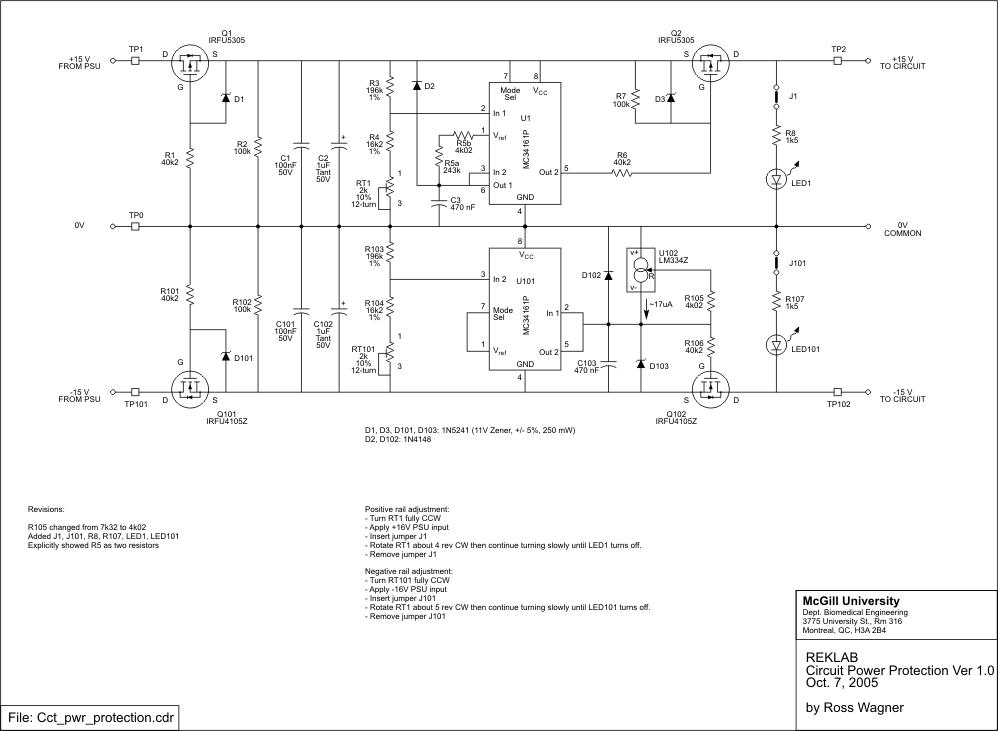
The above scematic is available in the original CorelDRAW 12 format and in PDF.
List of components
- IRFU4105Z N-channel enhancement MOSFET
- IRFU5305 P-channel enhancement MOSFET
- LM334Z 3-terminal adjustable current source
- MC34161P universal voltage monitor
- Parts List (Excel)
Functional Description
This circuit guards the power supply lines of circuitry downstream of
the main +/-15 V lab power supply unit (PSU). When this circuit board
is placed between the main PSU lines and the load circuit the load is
protected against overvoltage and reversal of +/- leads at the PSU. In
either condition the power is disconnected from the load circuit(*). The
overvoltage trip levels (one for each supply rail) are adjustable via
trimming potentiometers. (See schematic for instructions on how to set
overvoltage trip point.)
(*)The positive and negative supply rails are monitored independently.
Hence, in principle, the voltage on one rail may be allowed through to
the load circuit whereas the other may not.
Circuit Description
The circuitry above the 0V line monitors the positive rail. MOSFET Q1 is normally off and conducts when the voltage between the gate and source (VGS) is sufficiently negative. When a +15V power supply voltage is applied the body diode (between the drain and source) in Q1 conducts, bringing the voltage of the source above that of the gate, thus turning on the transistor. Hence, Q1 guards the load circuit against reversal of power polarity. Zener diode D1 and R1 clamp VGS to approximately -10V which is a safe level for Q1 while ensuring that Q1 is operating in full enhancement mode (i.e., ensuring that Q1 is fully 'on'.) Though D1 is nominally rated at 11V it is being operated at a very low reverse current (about 115 uA) due to R1. At this current the zener voltage is below the characteristic "knee" and is, therefore, less than the rated value.
U1 and surrounding components now have power to operate and the circuit to consider is shown below. RT1 is used to set the trip voltage during an overvoltage condition.
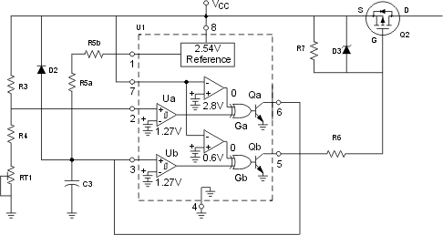
Under normal operating conditions the setting on RT1 causes the voltage at pin 2 of U1 to be less than 1.27V causing comparator Ua to output logical 0. XOR gate Ga then outputs a logical 0 and turns off transistor Qa, connected to pin 6. This places pin 6 in a high-impedance state. (Meaning that, apart from leakage current, the pin appears as an open circuit.) Meanwhile, U1's voltage reference pin (1) is charging capacitor C3 via R5a and R5b. Since pin 6 is (ideally) open-circuit it does not interfere with the charging process. While C3 is charging comparator Ub (at pin 3) is outputting logical 0. XOR gate Gb turns off transistor Qb, placing pin 5 in a high-impedance state as well. This keeps Q2 off since R7 keeps VGS = 0. The voltage across C3 is heading towards 2.54V; when it exceeds 1.27V the output of comparator Ub changes from logical 0 to 1 and turns on transistor Qb. This brings the gate of Q2 to nearly ground potential, biasing VGS negatively, turning on Q2, and applying power to the load circuit. Zener diode D3 limits VGS to approximately -10V for the same reasons mentioned when discussing Q1. Diode D2 allows C3 to discharge when main power is removed.
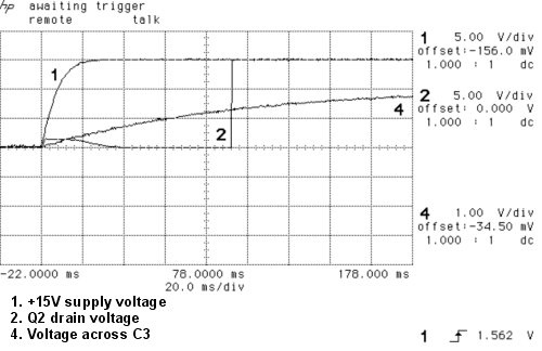
The oscilloscope screen shot below captures selected signals under normal operating conditions. The load circuit, in this case, is LED1 and R8.
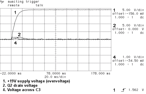
During an overvoltage condition, the potential at pin 2 exceeds 1.27V. This causes comparator Ua to output a logical 1 which turns on transistor Qa. This causes C3 to discharge and forces the voltage at pin 3 to be below 1.27V. Comparator Ub then outputs a logical 0 placing pin 5 in a high-impedance mode. This causes Q2 to turn off disconnecting power to the load circuit. The oscilloscope screen shot below captures selected signals under overvoltage operating conditions.
Referring to the main schematic at the top, the circuitry below the 0V line independently monitors the negative supply rail. Similar to above, the first MOSFET transistor (Q101) guards against reversal of supply polarity. Q101 is normally off and conducts when the voltage between the gate and source (VGS) is sufficiently positive. When a -15V power supply voltage is applied as shown the transistor-body diode conducts, making VGS largely positive, turning on the transistor. Zener diode D101 and R101 clamp VGS to a safe level of approximately 10V while ensuring that the transistor is operating in full enhancement mode. As mentioned above, the voltage developed across D101 is smaller than the rated zener voltage.
U101 and surrounding components now have power to operate and the circuit to consider is shown below. RT101 is used to set the trip voltage during an overvoltage condition.
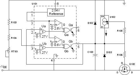
Under normal operating conditions the setting on RT101 causes the voltage at pin 3 to be more negative than -13.73V (= -15 + 1.27) causing the comparator Ub to output logical 0. XOR gate Gb then turns off transistor Qb putting pin 5 in a high-impedance state. (Pin 2 is an input and may be ignored.) If we assume that C103 is initially discharged then Q102 is off because its VGS = 0. Since U101 is effectively disconnected from C103 constant-current source U102 (programmed by R105) begins to charge the capacitor. After an initial startup transient, the voltage developed across C103 increases almost linearly with time. Q102 remains off until VGS reaches a threshold voltage (2 - 4V) at which point the device gradually turns on. Full turn-on is achieved when Q102 enters into an enhanced region (which is certainly the case when VGS = 10V.) Zener diode D103 limits VGS to a safe value of 10V. Hence, in the scale of milliseconds the load circuit sees the negative supply rail attain full level.When main power is removed D102 allows C103 to discharge.
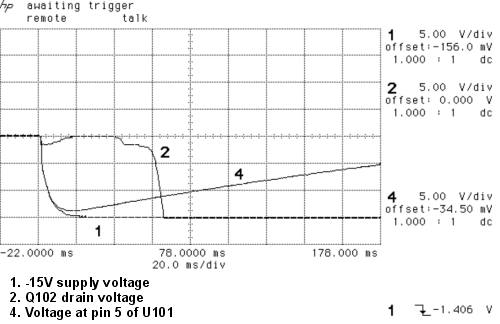
The oscilloscope screen shot below captures selected signals under normal operating conditions. The load circuit, in this case, is LED101 and R107.
The rate at which Q102 turns on is dependent upon the load current. R105 may have to be adjusted for a particular application so that both positive and negative supply rails appear to turn on at approximately the same time. Moreover, because the current generated by U102 is in the micro-ampere range leakage current through U101 (pins 2 and 5) and D102, and variable current through D103 necessitate that the current be set experimentally.
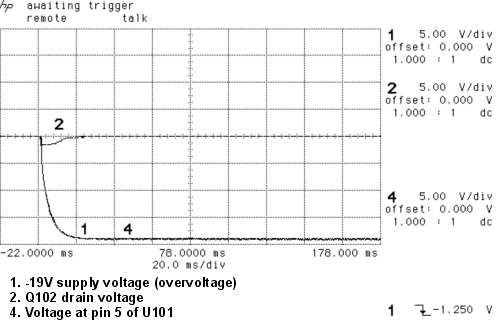
During an overvoltage condition, the potential at pin 3 is more positive than -13.73V. This causes comparator Ub to output a logical 1, consequently turning on Qb. C103 then discharges through Qb, bringing VGS to approximately 0V, turning off Q102, and disconnecting power to the load circuit. Diode D102 is normally reversed biased and plays no role in circuit operation. The oscilloscope screen shot below captures selected signals under overvoltage operating conditions.
All of the MOSFETs in the circuit tolerate a maximum of 55V across drain and source.
Printed Circuit Board
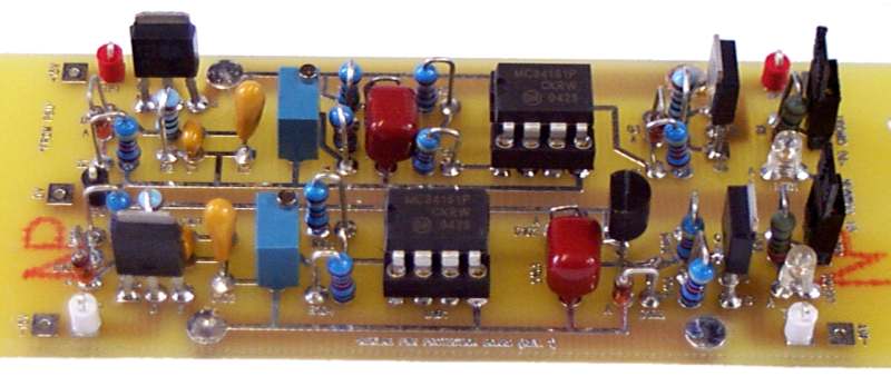
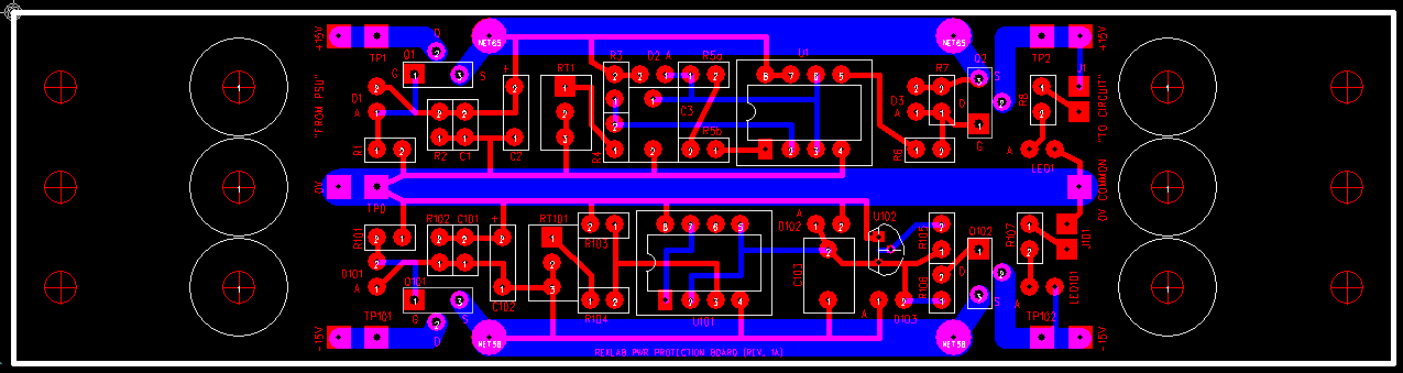
Click on the image for larger view.
Cick here for an image of
the PCB in PDF format.
Click here for the PCB source
file and associated application. (Zip file 6.64MB)
References
Dana Davis, "Overload and reverse-current circuitry protects battery and load." EDN Design Feature. EDN March 1, 1996. (web site)
Maxim Integrated Products, "Overvoltage protection in automotive systems." Application Note 760, June 18, 2001. (web site)
Last Modified: Jan 04, 2011 Ross Wagner