| Common apparatus |
|---|
| Hydraulic system |
| Electronic components |
| Data acquisition |
| EMG monitoring |
| NLID Tools |
| Troubleshooting |
| Materials |
| Supine apparatus |
|---|
| Assembly procedure |
| Safety Measures |
| Components |
| Servovalve |
| Actuator |
| Potentiometer |
| Pressure Filter |
| Torque transducer |
| Boot |
| Literature |
| Computing resources |
|---|
| CVS |
| Ethics |
|---|
| SDS / Inventory |
|---|
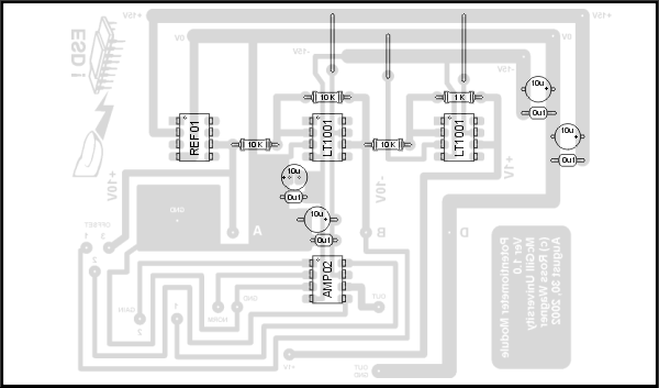
Potentiometer Module
Schematic
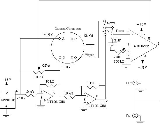
Components:
- LT1001 operational amplifiers
- REF01CP reference voltage source
- Cannon connector
- AMP02FP Instrumentation amplifier
- Variable resistors (trimpots)
- Resistors
- SP 3 position switches
- BNC connectors
Functional description
The purpose of this module is to condition the output of a potentiometer. The potentiometer measures the angular displacement of a wiper. This angular displacement is converted to a voltage between -10 and 10 volts (across pins A and C) in this module . The offset adjustment is used to set a known angle to a particular voltage. The gain adjustment is used to set the change in angle to a desired change in voltage. For example, a certain angle (say the ankle at neutral position) could be set to zero volts and an angular change of 90 degrees could be set to 9 volts. Therefore Vout=offset+gain*(deg/volt).
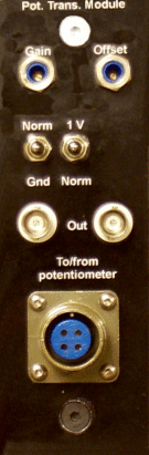
faceplate.cdr: CorelDRAW 9.0 file used to make faceplates
The switch settings for switch 1 are NORM and GND; for switch 2 they are 1V and NORM. The gain and offset of the input are adjusted via trim potentiometers. The minimum gain that can be set is 1.25 since the instrumentation amplifier has a gain of (50k ohms/x)+1, where x is a variable resistor of 200 K ohms.
To adjust the offset and gain:
- set switch 1 to GND
- adjust the offset trim pot to the desired value
- set switch 1 to NORM and switch 2 to1 V
- adjust the gain to the desired value
|
Switch 1 |
Switch 2 |
Output |
|
NORM |
1V |
gain setting |
|
NORM |
NORM |
Potentiometer input |
|
GND |
1V |
offset value |
|
GND |
NORM |
offset value |
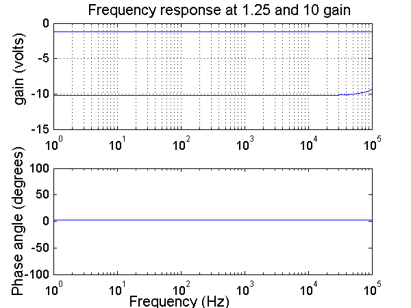
Frequency response
The frequency response at 2 different settings: gain of 1.25 or 10 and offset of 0 show a flat gain response and no phase shift. Note that the wiper is connected to the negative input of the instrumentation amplifier. Therefore the outputs are inverted.
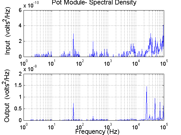
Noise Analysis
The output noise is very low for this module.
Printed Circuit Board
In order to make new printed circuit boards, use this pdf template. Alternatively, the PCB trace layout and component placement details may be found in the this CorelDraw 9 file.
Last modified: 2002-11-27 Ross Wagner