| Common apparatus |
|---|
| Hydraulic system |
| Electronic components |
| Data acquisition |
| EMG monitoring |
| NLID Tools |
| Troubleshooting |
| Materials |
| Supine apparatus |
|---|
| Assembly procedure |
| Safety Measures |
| Components |
| Servovalve |
| Actuator |
| Potentiometer |
| Pressure Filter |
| Torque transducer |
| Boot |
| Literature |
| Computing resources |
|---|
| CVS |
| Ethics |
|---|
| SDS / Inventory |
|---|
PSU Overvoltage Protection Module
Schematic
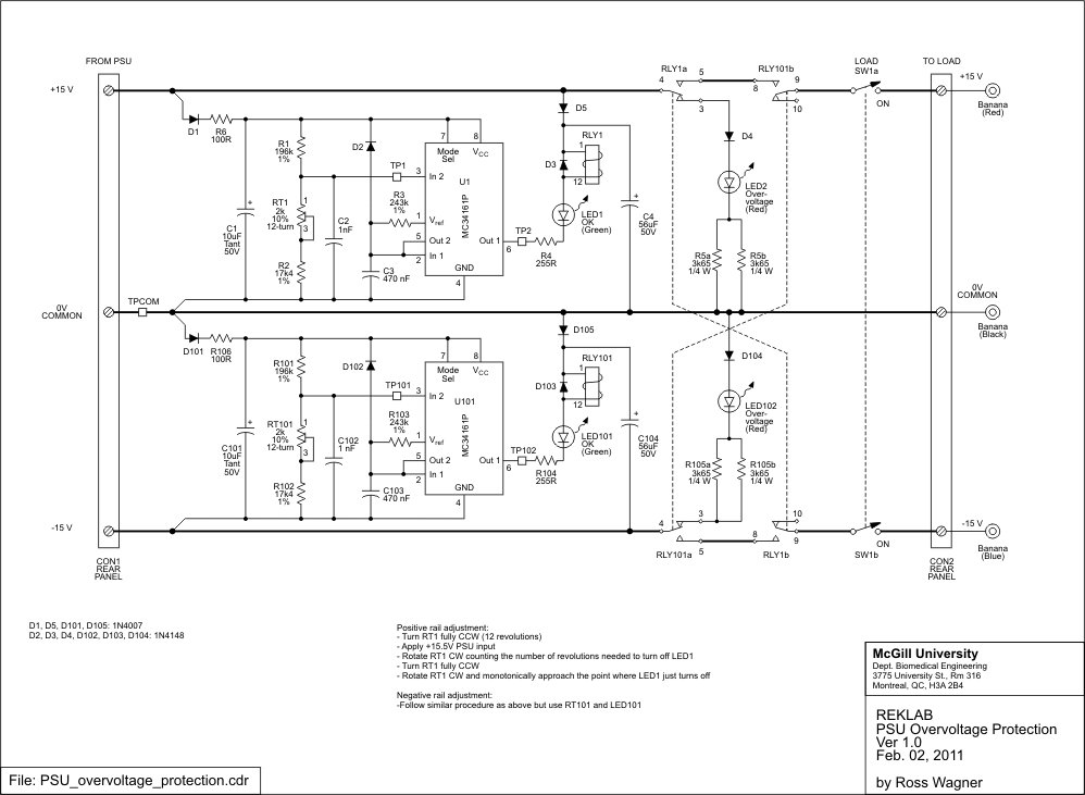
The above scematic is available in the original CorelDRAW 12 format and in PDF.
List of components
- MC34161P universal voltage monitor
- V23079A2003B301 Relay
- SSI-LXR4815GD Green LED
- SSI-LXR4815ID Red LED
- Parts List (Excel)
Functional Description
The module is located between the rack’s variable analog(*) power supply unit (PSU) and the rack’s power distribution panel (a plate with a multitude of banana jacks used to distribute power to the various chassis containing modules which, together, form the PSU ‘load.’) As such, the module protects the electronics downstream from overvoltage on the analog power supply lines by disconnecting the PSU from the load whenever the PSU voltage exceeds a threshold. The PSU is automatically reconnected to the load when the voltage levels fall below a prescribed threshold.
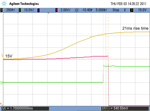
Upon powering up the PSU the monitor waits about 80ms to allow the PSU to power up to full voltage and then determines whether the voltage may be transferred to the load. (It typically takes ~35ms for the rack PSU to reach full voltage when it is set to +/- 15V.)
Though the positive and negative supply lines are independently monitored both are disconnected from the load during an overvoltage condition on either supply rail. The overvoltage trip level (one for each rail) is set via trimming potentiometers. (See the schematic for instructions on how to set the overvoltage trip point.)
The status of the voltage rails is indicated on the module front panel via LEDs. When either LED is red the load is not supplied with power.
A switch at the back of the module allows one to disconnect the load.
(*): The 5V digital rail is protected using the power supply's crowbar protection feature. Note that the crowbar level needs to be manually set.
Circuit Description
The circuitry monitoring the negative supply rail is identical to that used to monitor the positive rail. However, the circuit used for the positive supply may be easier to understand since the circuit common is conventional “ground,” while the reference potential for the negative supply monitor is the -15V line. As such, the negative-rail monitor circuit is awkward to test with single-ended oscilloscope measurements since the oscilloscope ground lead still needs to be connected to the ground (test point TPCOM) – which is the high side of that circuit. As such, the circuit will be explained using the positive rail monitor.
For the load to receive power both relays RLY1 and RL101 need to be activated and switch SW1 must be closed. By default the relays are not activated and power is routed to the overvoltage indicator LED2. (As such, when the PSU is initially turned on the overvoltage LED will momentarily light until the PSU voltage has built up to the level where the relays can be activated.)
Diode D1 guards against power supply lead reversal. D1 and C1 also implement a peak hold network, where the hold decays because charge is bled from C1. The significance of this is that switching transients can occur on the mains when a capacitive load is switched. One effect is that the mains voltage can momentarily drop when the load is switched in. (This will be demonstrated below.) The hold network stabilizes the power to U1 when the mains voltage dips. If C1 is too small then the relay will chatter (repeatedly close and open). R6 and C1 also form a low-pass filter that suppresses switching transients on the mains from reaching U1. This helps prevent brief overvoltage transients from triggering the protection circuitry. (C2 with surrounding resistors also filters the input to pin 3 but may be optional; certainly its effects are much less significant than the R6-C1 filtering.)
U1 and surrounding components now have conditioned power for operation. Circuit operation may be explained using the simplified schematic shown below.
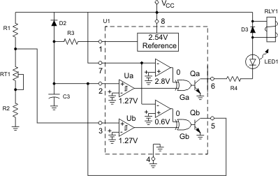
RT1 is used to set the trip voltage for the overvoltage condition. Under normal operating conditions the setting on RT1 causes the voltage at pin 3 of U1 to be less than 1.27V causing comparator Ub to output logical 0. XOR gate Gb then outputs a logical 0 and keeps transistor Qb off. This places pin 5 in a high-impedance state. (Meaning that, apart from leakage current, the pin appears as an open circuit.) R3 and C3 form a timing network to delay the activation of RLY1. U1's voltage reference pin (1) charges capacitor C3 via R3. Diode D2 is reversed biased (i.e., it is ideally open) and so does not interfere with the charging process nor does Qb. While C3 is charging comparator Ua (at pin 2) outputs logical 0. XOR gate Ga keeps Qa off, placing pin 6 in a high-impedance state as well. This prevents current from flowing through LED1 and RLY1 (so the green LED is off and the relay is not activated.) The voltage across C3 is increasing towards 2.54V; when it exceeds 1.27V the output of comparator Ua changes from logical 0 to 1 and turns on transistor Qa. This activates RLY1 and illuminates LED1. Diode D2 allows C3 to discharge after the PSU is turned off.
During an overvoltage condition, the potential at pin 3 exceeds 1.27V (perhaps even while C3 is charging up.) This causes comparator Ub to output a logical 1 which turns on transistor Qb. This causes C3 to discharge through Qb and forces the voltage at pin 3 to be below 1.27V. Comparator Ua then outputs a logical 0 placing pin 6 in a high-impedance mode which either turns off RLY1 (if already activated) or prevents RLY1 from activating (during PSU power-up.) Diode D3 is normally reversed biased and playes no role is circuit operation. It is there to squelch the back emf that is produced by RLY1 when it it deactivated. (Without D3 LED1 and U1 could be damaged.)
When a load is finally switched in the full 15V is applied to it. A capacitive load initially demands peak current from the PSU. When the demand is significant the PSU loses regulation and suddenly drops its output voltage. If the drop falls below the relay’s release voltage the relay will open and disconnect the load. At this point the circuit would start to chatter as the PSU recovers, increases its output voltage, only to see a capacitice load when the relay is again activated. D5 and C4 remedy this by creating an energy reservoir for the relay (see the main schematic.) While the PSU initially powers up the voltage across C4 follows the mains voltage (less the diode drop of ~650mV.) When the mains voltage level decreases D5 opens and the relay remains activated as long as the voltage across C4 does not droop below the relay’s release voltage, before the PSU has recovered. (Hence, the proper value of C4 is dependent upon the capacitive load.)
The figure below illustrates the effects of a capacitive load on the PSU and circuit. At 0ms the PSU is turned on: trace 1 shows that a steady +15V level is reached at ~35ms. At 84ms U1 determines to switch in the load: transistor Qa is turned on and the voltage at pin 6 drops to the transistor’s saturation voltage (see trace 2.) Approximately 5ms later RLY1 closes, switching in the load. The initial surge current causes the PSU voltage to drop from 15V to 3.2V (see trace 1). Trace 4 shows the voltage across C4 available to keep RLY1 active. While the mains supply is recovering from the effects of the surge current C4 is discharging but RLY1 remains activated since the voltage stays above the relay’s release voltage (1.2V).
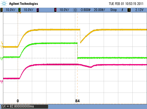 |
Load: 20ohm||1000uF (750mA dc current drain on PSU) Trace: |
The figure below shows the events that occur when an overvoltage condition exists. The PSU is initially set at +15V and the voltage-adjustment knob is turned rapidly to raise the mains. When the mains crosses the overvoltage threshold the current through the relay is interrupted (trace 2 goes up) and ~2ms later the relay deactivates (trace 4 goes down.)
 |
Load: 20ohm||1000uF Trace: Note different voltage sensitivity settings between traces. |
Printed Circuit Board
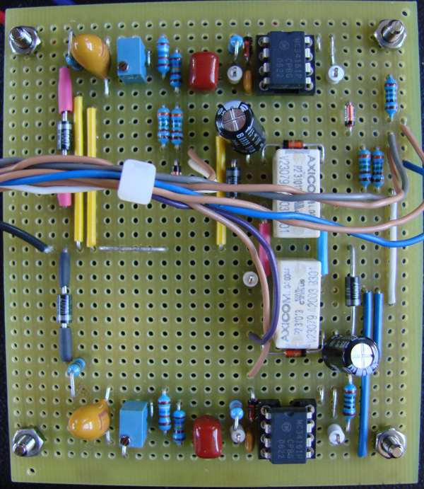
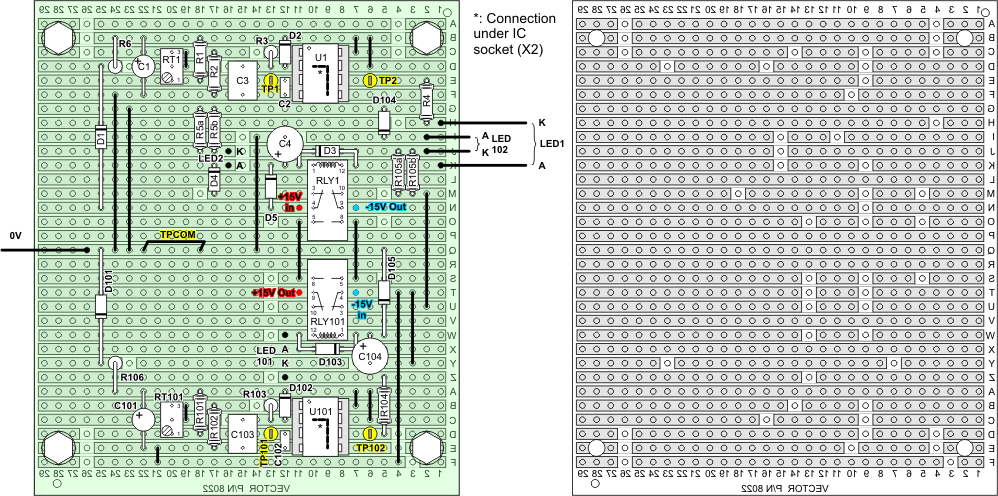
Click here for the circuit layout PDF format.
Click here for the circuit layout in original CorelDRAW format (v12).
Click here for the front/back panel layouts in original CorelDRAW format (v12).
Last Modified: Feb 03, 2011 Ross Wagner